Single Wire Signal Aggregation Demonstration

PCB Congestion Relief using FPGAs for Signal Aggregation and Transmission Over Single Wire

This solution is an FPGA bitstream that can be used to configure a Lattice FPGA to perform as a Single-Wire aggregator for I2C, I2S, and GPIO signalling. No FPGA design is needed. Two configured devices (denoted as Master Single-Wire Aggregation Device and Slave Single-Wire Aggregation Device) can be used to aggregate and deaggregate multiple signals on a single physical wire through Time Domain Multiplexing (TDM)-based bidirectional communication. Note: UART can be implemented using GPIO channel. Single Wire Signal Aggregation Demonstration – Two boards are provided to demonstrate the complete working design in a stand-alone configuration.

Features

  • No FPGA tools knowledge necessary
  • Customizable via available Reference Design
  • Up to 7 channels can be aggregated
  • Supports ultra-low power devices
  • Multiple sets of ready-to-use configurations to support different use case applications are available

Jump to

Videos

How to Setup SWA Demo

How to Run SWA Demo

Daisy-Chain Implementation of Single-Wire Signal Aggregation with Qualcomm RB5 Platform

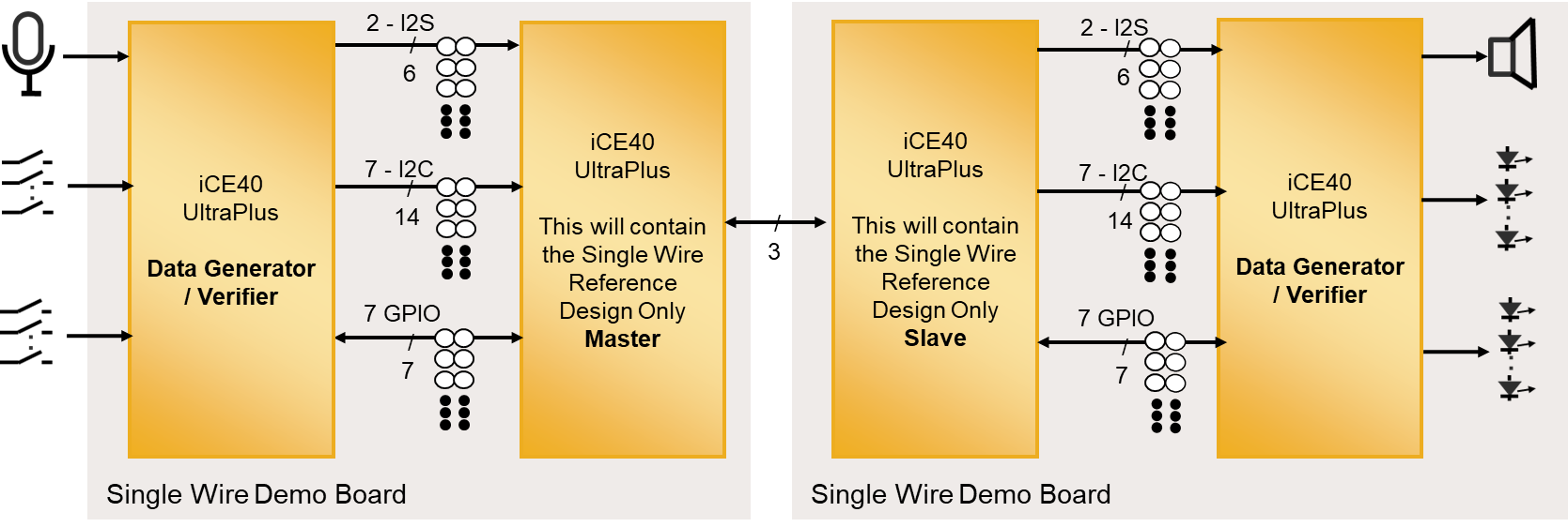
Block Diagram

Single Wire Signal Aggregation Demo/Dev Board – Block Diagram

  • Configurable for demonstration or prototyping
  • 12 Total Test Switches Available
  • Jumpers enable connection of RD to Data Generator/Verifier OR customer’s prototype
  • 12 output LEDs Available

Ready-to-Use Device Configurations Demo

Configuration #1 (I2Sx2_I2CSx1_I2CMx1_GPIOx8)

  • Two directional I2S channels (32 bits data width, 36 khz audio sampling)
  • One I2C Controller to Peripheral channel
  • One I2C Peripheral to Controller channel
  • 6 bits bidirectional GPIO channel
  • 2 bits bidirectional GPIO channel

Configuration #2 (I2CMx6_GPIOx6)

  • Six I2C Controller to Peripheral channels (at 400 khz SCL clock)
  • 6 bits bidirectional GPIO channel

Configuration #3 (I2CMx1_GPIOx12)

  • ONE I2C Controller to Peripheral Channel (at 1MHz SCL clock)
  • 12 bits bidirectional GPIO Channel

Configuration #4 (I2CMx3_I2CSx2_GPIOx15)

  • Three I2C Controller to Peripheral Channels
  • Two I2C Peripheral to Controller Channels
  • 15 bits Controller to Peripheral GPIO channel

Configuration #5 (I2Sx1_I2CMx1_I2CSx1_GPIOx8)

  • One directional I2S channels (32 bits data width, up to 48 khz audio sampling)
  • One I2C Controller to Peripheral channel
  • One I2C Peripheral to Controller channel
  • 6 bits bidirectional GPIO channel
  • 2 bits bidirectional GPIO channel

Documentation

Quick Reference
Downloads
TITLENUMBERVERSIONDATEFORMATSIZE
Select All
Single Wire Signal Aggregation User Guide
FPGA-UG-021171.15/1/2023PDF3.9 MB

*By clicking on the "Notify Me of Changes" button, you agree to receive notifications on changes to the document(s) you selected.

TITLENUMBERVERSIONDATEFORMATSIZE
Select All
Single Wire Signal Aggregation Demonstration - Bitstream
9/7/2020ZIP334.4 KB